Beacon Insights
April 9, 2026 10 min read
The Great AI Chip Bottleneck Shift: How Advanced Packaging Became the New
The AI chip supply chain crisis is undergoing a fundamental transformation.

Editorial Board
Editorial Board · Senior Columnist
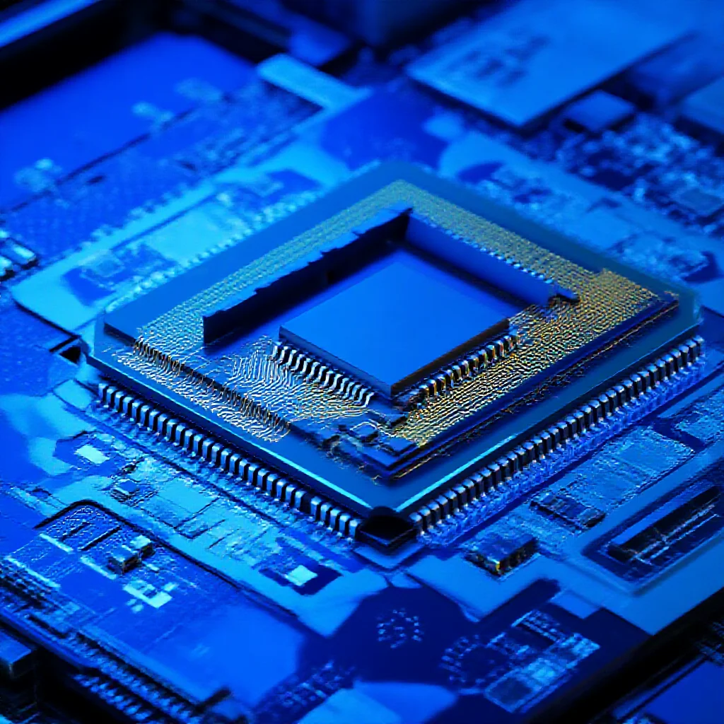
The Great AI Chip Bottleneck Shift: How Advanced Packaging Became the New Battleground
Introduction: The Stealthy Shift in the Semiconductor Bottleneck
For years, the primary constraint in the semiconductor supply chain was located at the front-end: the extreme ultraviolet (EUV) lithography process used to etch ever-smaller transistors onto silicon wafers. The narrative of scarcity centered on wafer starts and fab capacity. That paradigm has been decisively overturned. The critical bottleneck for artificial intelligence (AI) processors has migrated downstream to the back-end: advanced packaging. This is the complex, multi-step process of assembling and interconnecting discrete silicon chiplets—including processors and high-bandwidth memory (HBM)—into a single, functional unit. This shift redefines industry power dynamics, competitive strategy, and the technical definition of core manufacturing competency in the AI hardware era.The Nvidia Gambit: Securing the New Strategic High Ground
The most consequential evidence of this shift is a single strategic maneuver. Nvidia has locked in a large share of TSMC's CoWoS (Chip-on-Wafer-on-Substrate) advanced packaging capacity for 2025 and 2026 (Source 1: [Primary Data]). This is not merely a large purchase order; it is a calculated move to control the new critical path in AI chip production. By securing this capacity, Nvidia has erected a formidable supply chain moat that extends beyond its architectural design prowess. The immediate implication is a constriction of available CoWoS capacity for competitors. Companies like AMD, for its MI-series accelerators, and Intel, for its Gaudi line, are consequently forced to seek alternative packaging solutions, potentially delaying product roadmaps or limiting scale.Beyond CoWoS: Why Packaging is the New Frontier
Advanced packaging has evolved from a protective afterthought to a core performance differentiator. For AI workloads, performance is gated by memory bandwidth and the interconnectivity between specialized processing chiplets and HBM stacks. Technologies like TSMC's CoWoS enable this dense integration, acting as the essential plumbing for data. The innovation race has therefore expanded from a singular focus on transistor scaling (Moore's Law) to a parallel competition in "heterogeneous integration" (the ability to combine disparate chiplets). This has elevated packaging R&D to a strategic priority, with TSMC, Intel (with its EMIB and Foveros technologies), and Samsung all pushing distinct roadmaps. The performance of an AI accelerator is now as dependent on its package as on the transistors inside it.The Ripple Effect: Reshaping the Competitive Landscape
The Nvidia-TSMC dynamic has triggered a scramble that is reshaping the semiconductor competitive map. The search for alternative packaging capacity is accelerating the evaluation and adoption of competing technologies. Intel, for instance, is now positioned not only as a chip designer and foundry but also as a potential advanced packaging provider for third parties via its Intel Foundry Services. This bottleneck may inadvertently foster a more multi-polar packaging ecosystem. However, it also highlights a deepening systemic concentration risk. The industry's dependence on TSMC for both leading-edge wafer fabrication and the dominant form of advanced packaging creates a single point of potential failure. Competitors and customers are incentivized to diversify, but viable, high-volume alternatives remain in development.The Deep Audit: Long-Term Implications for the Global Supply Chain
This bottleneck shift signals a fundamental transition from a "vertical scaling" model—making a single chip faster—to a "horizontal scaling" and integration model. The long-term implications are structural. First, capital expenditure is being redirected. TSMC is expanding its CoWoS capacity, with projections indicating it will more than double from 2024 levels by the end of 2025 (Source 2: [Primary Data]). Second, the definition of a semiconductor manufacturing leader is expanding to require mastery over both front-end and back-end processes. Third, supply chain resilience strategies must now account for packaging as a tier-one risk, equivalent to wafer fab location and equipment availability. The ability to secure and integrate advanced packaging will be a primary determinant of market share in the AI hardware sector for the foreseeable future.Conclusion: Packaging as the Pivot Point of AI Hardware Supremacy
The relocation of the AI chip bottleneck to advanced packaging represents a permanent recalibration of the semiconductor industry. Control over this process has become as strategically valuable as control over chip design. Nvidia's capacity lock exemplifies this new reality. The competitive response will dictate the next phase of the industry, potentially leading to a fragmentation of packaging standards or the rise of new foundry-packaging hybrids. One conclusion is inescapable: in the race for AI compute supremacy, the package is now the pivot point. The companies that master the art and science of silicon assembly will hold decisive leverage over the pace and direction of AI hardware development.(All rights reserved by Global Beacon Chronicle. Unauthorized reproduction is prohibited.)
Editorial Board / Editorial Board
Collective pseudonym for the Global Beacon Chronicle editors.
#AI chip
#advanced packaging
#supply chain bottleneck
#TSMC CoWoS
#Nvidia
#semiconductor
#chiplet
#AMD
#Intel